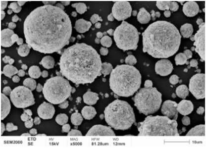
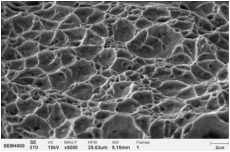
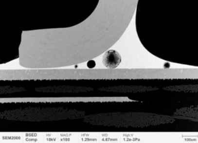
The scanning electron microscopy uses a small focused high-energy electron beam to scan the surface of the device, and uses various signals excited by the interaction between electron beams and matter to image, such as secondary electrons, backscattered electrons, characteristic x-rays, etc. Due to its characteristics such as large depth of focus, high resolution and high magnification, it can be used to observe the micro-structure of the surface and section of devices.
Application
Integrated Circuits, Transistors, Resistors, Capacitors, Inductors, Transformers, Sensors, Electromechanical Components, Connectors, PCB, PCBA, Power Modules, Signal Modules, Organic Components, etc